-
Technology
-
Industry
-
Solutions
-
- ASSET MANAGEMENT
- CUSTOMER EXPERIENCE MANAGEMENT
- CYBER SECURITY
- DATA CENTER
- DOCUMENT MANAGEMENT
- ELECTRONIC DATA INTERCHANGE
- ENTERPRISE DATA MANAGEMENT
- ENTERPRISE RESOURCE PLANNING
- ENTERPRISE RISK MANAGEMENT
- ENTERPRISE-GRADE WEB DATA SOLUTIONS
- FACILITY MANAGEMENT
- FIELD SERVICE
- IDENTITY AND ACCESS MANAGEMENT
- INFRASTRUCTURE
- IT SERVICE MANAGEMENT
- MANAGED IT SERVICES
- PAYMENT AND CARD
- PROJECT MANAGEMENT
- SOFTWARE TESTING
- STORAGE
- VIDEO SOLUTIONS
- WORKFLOW
-
-
Platforms
-
Functions
- Leadership Perspectives
- Innovation Insights
- Research
- Magazines
- News
- CXO Awards


 Andy Hsu, Founder and CEO
"X-NAND is an 'Enhanced Version' of NAND flash memory that can significantly improve the read and write speeds of NAND flash memory without adding cost"
In parallel with these developments, the current industry trend is to add a buffer layer called Storage Class Memory (SCM) between the NAND flash memory and the system. SCM uses new types of memory technologies such as phase-change memory (PCM) or resistive random-access memory (RRAM) to bridge the gap between traditional memory and storage and change how data is processed and stored. Experts often opine that this specific type of memory is driving the future of storage. But, it requires new manufacturing processes and materials for which the die cost can be up to five times that of traditional NAND.
This is where NEO Semiconductor steps in with its unique solution.

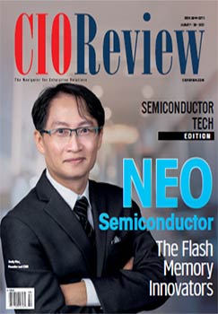
Established in 2012, NEO Semiconductor specializes in 3D NAND flash memory technology. The company's X-NAND technology is a game-changer in the industry as it transforms the NAND flash memory architecture itself instead of developing a new type of memory. "X-NAND is an 'Enhanced Version' of NAND flash memory that can significantly improve the read and write speeds of NAND flash memory without adding cost. It can be quickly implemented in the next NAND flash products without changing the manufacturing process," says Andy Hsu, Founder and CEO, NEO Semiconductor.

The innovative circuit design allows the die size of X-NAND to remain the same or smaller compared to conventional NAND flash memory. More importantly, this architecture can be implemented in existing NAND flash memory products without changing any manufacturing process.
This is a crucial factor in minimizing the development time, cost, and risk. "We have designed a new architecture that divides the NAND flash memory array into multiple (8 – 64) small planes. This can increase both the random read and write speeds by 3X, as well as the sequential read and write speeds by 30X and 15X.," states Hsu.NEO Semiconductor currently owns 20 U.S. patents in memory design architectures and cell structures.
We have designed a new architecture that divides the NAND flash memory array into multiple (8 – 64) small planes. This can increase both the random read and write speeds by 3X, as well as the sequential read and write speeds by 30X and 15X

'Enhanced Version' of NAND Flash Memory
According to Hsu, the conventional NAND flash memory's performance is limited by the number of page buffers. To read and write data, each bit line needs to be connected to one 'page buffer' circuit. The page buffers' layout size is very large. For 1Tb NAND flash products using Circuit under Array (CUA) structure, the array is divided into 4 planes with each plane requiring 16KB page buffers. The total 64KB page buffers' layout occupies about 50 percent of the die size, so the page buffer size cannot be increased without significantly increasing the die size.
Unlike this, NEO Semiconductor's X-NAND architecture allows one page buffer to control multiple bit lines. Therefore, it can increase the number of planes up to 64 without increasing the page buffer size. This allows 16X of data to be read and programmed simultaneously to increase the data throughput while reducing the bit line length to 1/16 and the bit line capacitance and bit line latency to only 1/16.

X-NAND architecture can also be applied to SLC for serial NAND flash memory, which consists of the operating system and firmware of the processor and modules and the program and data that the programmer uses. Simulations show TLC's read time and write time can be reduced to 20us and 200us, respectively. Further, QLC's random read time and write time can be reduced to 25us and 550us. These speed performances are comparable to SLC. The die cost of TLC and QLC is about 1/3 and 1/4 of SLC, respectively.
As a result, X-NAND can provide SLC-comparable high speed and TLC and QLC-comparable low cost. This provides an excellent solution for the booming markets of 5G, AI, and IoT applications.
Besides being used in cloud storage and data centers (TLC and QLC), X-NAND can also be implemented in embedded systems such as image-based AI applications. These applications require low latency and high throughput to execute the AI algorithm stored in the flash memory.
 Ray Tsay, Co-founder & VP of Engineering
An IP solution for NAND Flash Companies
Being an IP design house, NEO Semiconductor provides X-NAND architecture as an IP solution to NAND flash companies to replace the traditional NAND flash memory design."We are proud of the fact that NEO Semiconductor is the only company offering such a robust solution. This provides us with a strong and unique position in the market," mentions Hsu.
In the past 20 years, many companies have invested a significant amount of money in researching and developing emerging technologies such as PCM, RRAM, MRAM, and FRAM in an attempt to replace NAND flash memory. However, till today, all technologies have been re-targeted to SCM or embedded memory markets due to the high cost of these emerging memories. NAND flash memory still dominates the data storage market, and its reign will not end anytime soon. That's why NEO Semiconductor plans to work with multiple major NAND flash memory companies to provide solutions for both data storage (TLC – QLC) and IoT embedded system markets (SLC). "Our X-NAND architecture solves the speed issue of NAND flash memory by increasing the planes of the array and using the existing page buffer size. This increases the parallelism for the 'read and write' operations. As a result, X-NAND can achieve QLC density with SLC speed," Hsu mentions.

NEO Semiconductor's unique capabilities have helped the company won multiple awards, including the Flash Memory Summit's 'Best of the Show' Award for 'Most Innovative Flash Memory Startup' of 2020. Jay Kramer, Chairman of the Awards Program and President of Network Storage Advisors Inc., mentions, "We are proud to recognize NEO Semiconductor's X-NAND product solution for providing an excellent high-performance solution that can uniquely lower the cost across all tiers of SSD technologies." According to Hsu, "the recognition was a fantastic honor and achievement for the debut of X-NAND."
Developing Advanced Technologies for Semiconductor Field
NEO Semiconductor is on the high growth path today. "X-NAND is our first technology announced to the industry. We are currently preparing the promotion of X-NAND technology to potential licensees and partners. Our goal is to start the sample chip development in 2022 and move X-NAND into production in 2023," informs Hsu.

NEO Semiconductor does not stop there! It is also working on advanced technologies in other fields and with new announcements in the pipeline. "Our goal is to work with major semiconductor companies to bring these wonderful technologies into the world and benefit our everyday life. We believe we will get there," concludes Hsu.
NEO Semiconductor to Present its 3D X-AI, Game-changing 3D Memory with AI Processing, in Keynote Address at FMS 2024: the Future of Memory and Storage
Thursday, July 18, 2024
CEO Andy Hsu will introduce NEO Semiconductor's 3D X-AI™, a game-changing 3D memory with AI processing that combines data storage and data processing in a single chip, accelerating neural performance by 100X and reducing power consumption by 99%
SAN JOSE, Calif.,-- NEO Semiconductor, a leading developer of innovative technologies for 3D NAND flash and DRAM memory, today announced its participation at FMS 2024: the Future of Memory and Storage, taking place in person in Santa Clara, California, on August 6-8. CEO, Andy Hsu, will deliver a keynote address titled "New 3D AI Chip Technology Accelerates Generative AI" on August 6th at 11:45 a.m. Pacific Time.
Based on NEO's award-winning 3D X-DRAM™ technology, 3D X-AI simulates artificial neural networks (ANNs), including synapses for weight data storage and neurons for data processing, making it ideally suited to accelerate next-generation AI chips and applications. 3D X-AI substitutes for high-bandwidth memory (HBM) and is expected to significantly evolve AI chip design and AI workload optimization. A single 3D X-AI die includes 300 layers of 3D memory with 128 Gb (gigabit) capacity and 1 layer of neural circuitry with 8,000 neurons supporting up to 10 TB/s (terabytes per second) of AI processing throughput per die. Using twelve 3D X-AI dies stacked with HBM packaging can scale 3D X-AI chip capacity and performance by 12X to reach 1,536 Gb (192 GB) capacity and 120 TB/s processing throughput with a single 3D X-AI chip.
"Typical AI chips use processor-based neural networks. This involves combining high-bandwidth memory to simulate synapses for storing weight data and graphical processing units (GPUs) to simulate neurons for performing mathematical calculations. Performance is limited by the data transfer between HBM and GPU, with back-and-forth data transfer lowering AI chip performance and increasing power consumption," said Andy Hsu, Founder & CEO of NEO Semiconductor. "AI chips with 3D X-AI use memory-based neural networks. These chips possess neural network functions with synapses and neurons in each 3D X-AI chip. They are used to drastically reduce the heavy workload of data transfer data between GPU and HBM when performing AI operations. Our invention drastically improves AI chip performance and sustainability".

Company
Neo Semiconductor
Management
Andy Hsu, Founder and CEO and Ray Tsay, Co-founder & VP of Engineering
Description
Established in 2012, NEO Semiconductor specializes in 3D NAND flash memory technology. The company's X-NAND technology is a game-changer in the industry as it transforms the NAND flash memory architecture itself instead of developing a new type of memory. NEO Semiconductor's X-NAND architecture allows one page buffer to control multiple bit lines. Therefore, it can increase the number of planes up to 64 without increasing the page buffer size. This allows 16X of data to be read and programmed simultaneously to increase the data throughput while reducing the bit line length to 1/16 and the bit line capacitance and bit line latency to only 1/16